
CG635时钟发生器
CG635产生极为稳定频率范围从1μHz到2.05GHz的方波时钟。该仪器具有高频率分辨率,低抖动,快速转换时间和灵活的输出电平等特点使之成为任何数字元件、系统或网络测试的最理想选择。
·时钟频率1μHz到2.05GHz
·随机抖动<1 ps rms
·16位频率分辨率
·80 ps的上升和下降时间
·CMOS,PECL,ECL,LVDS,RS - 485的输出
·相位控制和时间调制
·OCXO的和铷时基(选配)
CG635产生极为稳定频率范围从1μHz到2.05GHz的方波时钟。该仪器具有高频率分辨率,低抖动,快速转换时间和灵活的输出电平等特点使之成为任何数字元件、系统或网络测试的最理想选择。
·时钟频率1μHz到2.05GHz
·随机抖动<1 ps rms
·16位频率分辨率
·80 ps的上升和下降时间
·CMOS,PECL,ECL,LVDS,RS - 485的输出
·相位控制和时间调制
·OCXO的和铷时基(选配)
CG635
The CG635 generates extremely stable square wave clocks between 1 µHz and 2.05 GHz. The instrument's high frequency resolution, low jitter, fast transition times, and flexible output levels make it ideal for use in the development and testing of virtually any digital component, system or network.
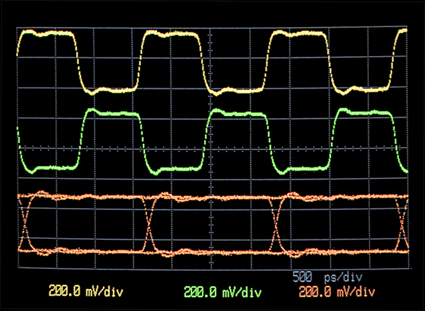
 Clock and PRBS Signals |
Clean clocks are critical in systems that use high-speed ADCs or DACs. Spurious clock modulation and jitter create artifacts and noise in acquired signals and in reconstructed waveforms. Clean clocks are also important in communications systems and networks. Jitter, wander, or frequency offsets can lead to high bit error rates, or to a total loss of synchronization. The CG635 can provide the clean, stable clocks required for the most critical applications.
Output Drivers
The CG635 has several clock outputs. The front-panel Q and
The front-panel CMOS output provides square waves at standard logic levels. The output may also be set to any amplitude from 0.5 V to 6.0 V. The CMOS output has transition times of less than 1 ns and operates up to 250 MHz. It has a 50 Ω source impedance and is intended to drive high impedance loads at the end of any length of 50 Ω coax cable.
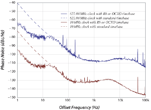
 Phase Noise |
A rear-panel
Choice of Timebases
The standard crystal timebase has a stability of better than 5 ppm. The CG635's 10 MHz timebase input allows the instrument to be phase-locked to an external 10 MHz reference. The 10 MHz output may be used to lock two CG635s together.
There are two optional timebases.
Phase and Time Modulation
The clock phase can be adjusted with high precision. The phase resolution is one degree for frequencies above 200 MHz, and increases by a factor of ten for each decade below 200 MHz, with a maximum resolution of
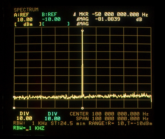
 RF Spectrum of a 100 MHz Clock |
The timing of clock edges can be modulated over ±5 ns via a
For Every Application
With its exceptionally low phase noise and high frequency resolution, the CG635 replaces RF signal generators in many applications.
The CG635 can provide a wide range of clean, precise clocks for the most critical timing requirements. The instrument is an essential tool for demonstrating a system's performance with a nearly ideal clock, and for understanding a system's susceptibility to a compromised clock. The CG635 has the frequency range, precision, stability, and jitter-free performance needed to fulfill all your clock requirements.
CG635 Specifications
Frequency
RangeDC, 1 µHz to 2.05 GHz
Resolution16 digits (f ≥ 10 kHz), 1 pHz (f < 10 kHz)
AccuracyΔf < ±(2 × 10-19 + timebase error) × f
Settling time<30 ms
Timebase (20 °C to 30 °C ambient)
Stability<5 ppm (std. timebase)
<0.01 ppm (opt. 02 OCXO)
<0.0001 ppm (opt. 03 Rb timebase)
Aging<5 ppm/year (std. timebase)
<0.2 ppm/year (opt. 02 OCXO)
<0.0005 ppm/year (opt. 03 Rb timebase)
External input10 MHz ± 10 ppm, sine >0.5 Vpp, 1 kΩ
Output10 MHz, 1.41 Vpp sine into 50 Ω
Phase Noise (at 622.08 MHz)
100 Hz offset<-90 dBc/Hz
1 kHz offset<-100 dBc/Hz
10 kHz offset<-100 dBc/Hz
100 kHz offset<-110 dBc/Hz
Jitter and Wander
Jitter (rms)<1 ps (1 kHz to 5 MHz bandwidth)
Wander (p-p)<20 ps (10 s persistence)
Time Modulation (rear-panel input)
Input impedance1 kΩ
Sensitivity1 ns/V, ±5 %
Range±5 ns
BandwidthDC to greater than 10 kHz
Phase Setting
Range±720° (max. step size ±360°)
Resolution<14 ps
Slew time<300 ms
Q and −Q Outputs
OutputsFront-panel BNC connectors
Frequency rangeDC to 2.05 GHz
High level-2.00 V ≤ VHIGH ≤ +5.00 V
Amplitude200 mV ≤ VAMPL ≤ 1.00 V
(VAMPL ≡ VHIGH - VLOW)
Level resolution10 mV
Level error<1 % + 10 mV
Transition time<100 ps (20 % to 80 %)
Symmetry<100 ps departure from nominal 50 %
Source impedance50 Ω(±1 %)
Load impedance50 Ω to ground on both outputs
Preset levelsPECL, LVDS, +7 dBm, ECL
CMOS Output
OutputFront-panel BNC
Frequency rangeDC to 250 MHz
Low level-1.00 V ≤ VLOW≤ +1.00 V
Amplitude500 mV ≤ VAMPL ≤ 6.00 V
(VAMPL ≡ VHIGH - VLOW)
Level resolution10 mV
Level error<2 % of VAMPL+ 20 mV
Transition time<1 ns (20 % to 80 %)
Symmetry<500 ps departure from nominal 50 %
Source impedance50 Ω (reverse terminates cable reflection)
Load impedanceUnterminated 50 Ω cable of any length
Attenuation (50 Ω load)Output levels are divided by 2
Preset levels1.2 V, 1.8 V, 2.5 V, 3.3 V or 5.0 V
RS-485 Output
OutputRear-panel RJ-45
Frequency rangeDC to 105 MHz
Transition time<800 ps (20 % to 80 %)
Clock outputPin 7 and pin 8 drive twisted pair
Source impedance100 Ω between pin 7 and pin 8
Load impedance100 Ω between pin 7 and pin 8
Logic levelsVLOW = +0.8 V, VHIGH = +2.5 V
Recommended cableStraight-through Category-6
LVDS Output (EIA/TIA-644)
OutputRear-panel RJ-45
Frequency rangeDC to 2.05 GHz
Transition time<100 ps (20 % to 80 %)
Clock outputPin 1 and pin 2 to drive twisted pair
Source impedance100 Ω between pin 1 and pin 2
Load impedance100 Ω between pin 1 and pin 2
Logic levelsVLOW = +0.96 V, VHIGH = +1.34 V
Recommended cableStraight-through Category-6
PRBS (Opt. 01, EIA/TIA-644)
OutputsPRBS, -PRBS, CLK and -CLK
Frequency rangeDC to 1.55 GHz
LevelLVDS on rear-panel SMA jacks
PRBS generatorx7 + x6 + 1 for a length of 27 - 1 bits
Transition time<100 ps (20 % to 80 %)
Load impedance50 Ω to ground on all outputs
General
Computer interfacesGPIB and RS-232 std. All functions can be controlled through either interface.
Non-volatile memoryTen sets of instrument configurations can be stored and recalled.
Power90 to 264 VAC, 47 to 63 Hz, 50 W
Dimensions, weight8.5"× 3.5" × 13" (WHL), 9 lbs.
WarrantyOne year parts and labor on defects in materials and workmanship


